Problem Statement
This project was created to facilitate the ease of use of our recently acquired inverter, the PM100DX-SP. Like our previous inverter, the PM100DX-SP contains multiple input and output pins. The inverter uses a 35 pin and a 23 pin AMPSEAL connector. While a few pins are never used, it was necessary to provide breakouts for the pins that are being used. Using these ideas, the scope of the project was determined. What we wanted this board to do was keep all the low voltage circuits pertaining to the inverter on one board and provide breakouts to pins as necessary.
Constraints and Criteria
In addition to the scope, there are a few constraints that have been used when designing. The biggest constraint was that the breakout board needed to be compact. In addition to being compact, the board needed to be relatively inexpensive. These two constraints were the major factors for the design of this board.
There are a few criteria that would make the breakout board considered good. Being a new part that is going on the car, the breakout board cannot be directly compared against another board. Due to this, the criteria chosen for this board relate to the constraints. The most important factor that was considered was that this board should allow for easy diagnostics. In addition, the board should group like components together to further assist with debugging. Overall, this board should be easier to use with our new inverter.
Solution
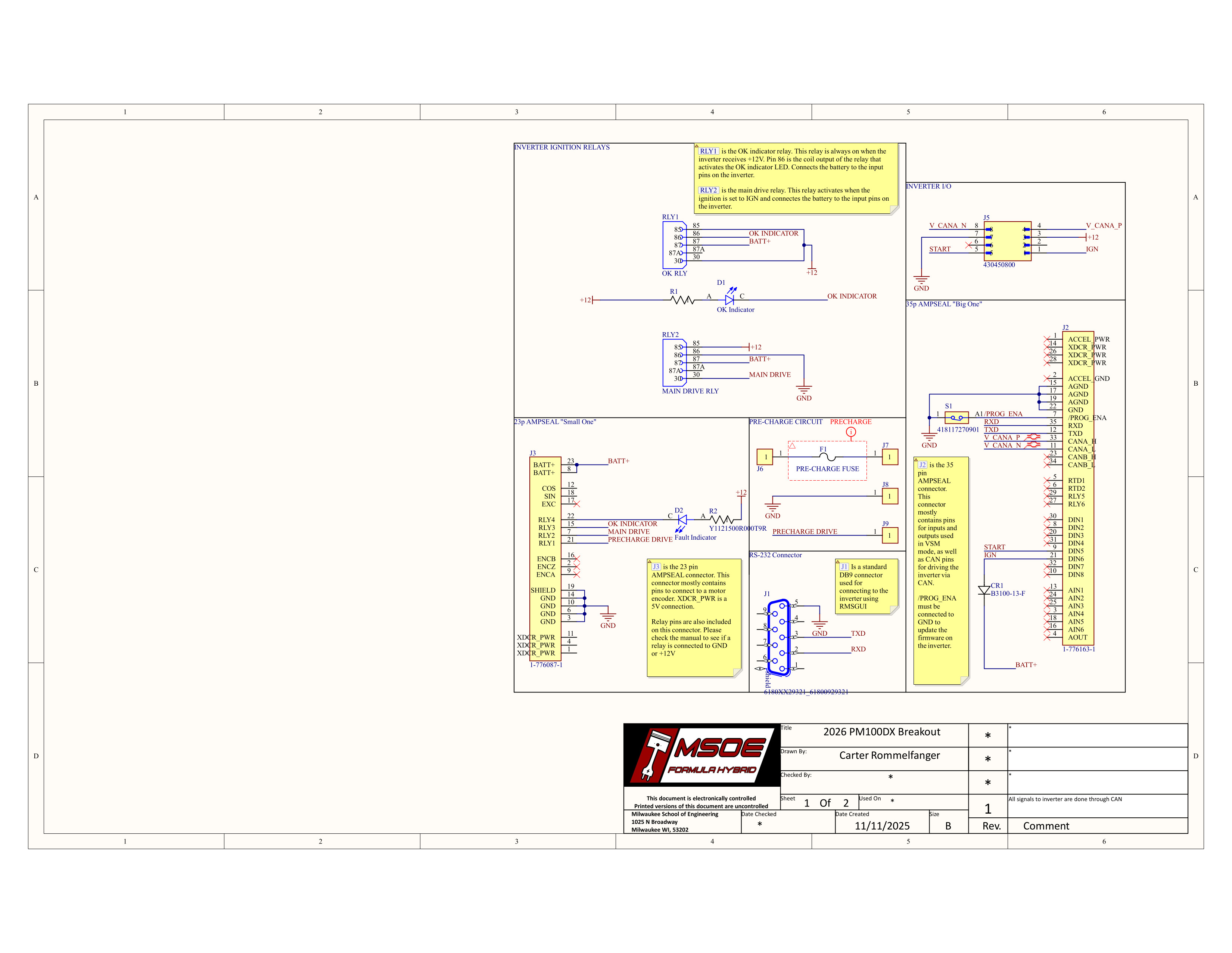
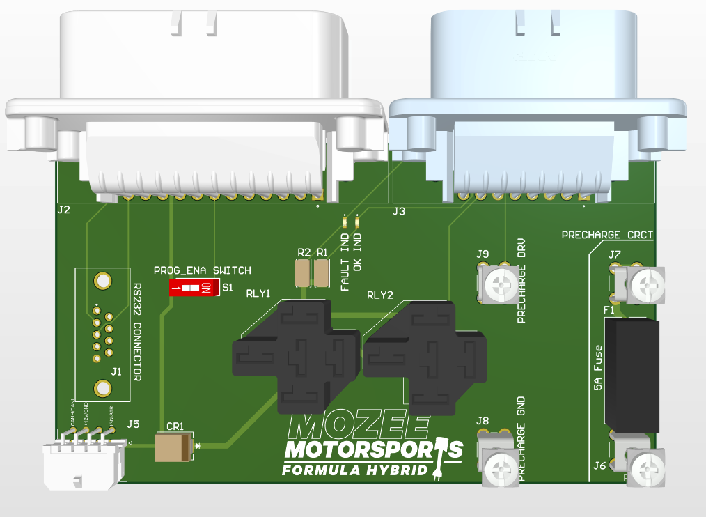
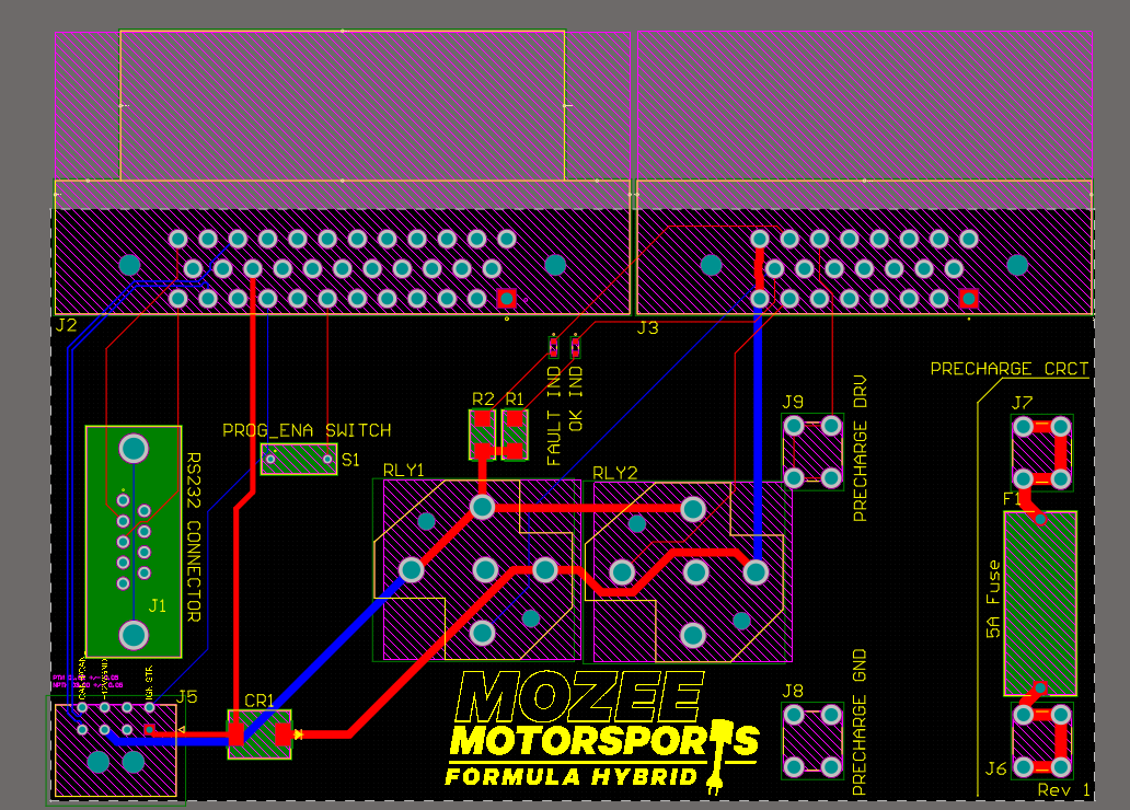
The final solution to the breakout board (BOB) is shown in the images above. The inverter needs three major components in addition to the regular breakout points to function properly. The first and most important component is a 12-volt supply and ground. This is utilized throughout the entire PCB and plays a role in using the ignition-start mode of the inverter. Currently, the +12V comes in from the bottom left of the top side of the PCB and goes into a relay and a pin on the inverter. This pin is the ignition pin, and it is what acts as if a key on a car has been turned to ignition; the inverter does not fully activate at this point. The relay is described by Cascadia Motion as the “OK” relay. This relay is supposed to provide power to the inverter even when the key is switched off. This allows the inverter to gracefully shutdown instead of being forced off due to a lack of power. As of right now, this relay is not being used due to a few mistakes being made during the creation of this board. This means that the inverter is in a simple “on-off” mode where providing it power turns it on and removing that power turns it off. The second component needed for the inverter is access to RS-232, which provides an access point to program the parameters on the inverter. This currently works as intended. Next, the third component needed is access to the inverter’s CAN pins. There are two pins, CAN high and CAN low. These are differential pairs that allow multiple devices to communicate with each other. As of right now CAN is the only method of controlling the inverter (i.e. send a command to rotate the motor shaft). There are a few more things to address regarding the functionality of the BOB.
One component on this board is currently non-functional. This component is the “Main Drive Relay,” designated as RLY2. Due to a few mix-ups that occurred during the design process, this relay was originally intended to act as a fault relay, which activates on and off in a pattern, like morse code, that allows one to determine what fault has occurred. This was mistaken for the main drive relay, which is intended to be the main contactor to allow high voltage power to flow into the inverter. This led to the inverter being powered when it was not supposed to. The output of this relay was connected to the main drive relay pin on the inverter, which is activated by the inverter when it wants to turn on the main contactor. Sending 12 volts into this pin provided power to the inverter unintentionally, which created confusion when the inverter did not turn on when this relay was removed, even when it was supposed to. Eventually, the problem was resolved, leading to the removal of this relay. This component is the only component on the BOB to be removed. The pin that activates the main contactor was soldered directly to the coil of the main contactor. Overall, the BOB does what it was designed to do.
There are a few non-necessary breakouts that were put onto the BOB. Two of these breakouts are terminals J8 and J9, labeled “precharge gnd” and “precharge drv” respectively. These breakouts are intended to provide easy access to close the pre-charge relay. The pre-charge relay is a part of the pre-charge sequence on the inverter, and it allows 72 volts to flow through a 600-ohm power resistor, which then goes through a 5-amp fuse. This leads to the other two breakouts on the BOB. The terminal connectors designated as J6 and J7 allow this 5-amp fuse to be utilized during the pre-charge sequence. Including these non-necessary breakouts, the BOB currently performs mostly as intended and achieves all the goals, criteria, and constraints that were set during the design process.
Risk Assessment
Overall, the breakout board (BOB) is not a high-risk design. This does not mean that there are no risks involved when utilizing the BOB. There is currently one problem-point for this board. As stated earlier, there is a 5-amp fuse that is used in the pre-charge sequence. This fuse, during the pre-charge sequence could potentially have greater than 72 volts going through it. While not being connected to anything else, it is isolated and separate from the other components on the board, there is a potential for it to short to a pin on the inverter (i.e. if a piece of metal falls onto it, which should not happen due to the BOB being enclosed in a tight container). Depending on the pin, this could permanently damage the inverter. This event has a non-zero chance of happening. If changes were to be made to this board, these breakouts could be modified to make this slightly less likely to happen.